联系人: 井 旭
电话: 0531-88153122
手机: 13791139332
邮箱 : jingxu@coupletech.com
地址: 济南市历城区华信路15号C座1楼
传真: 0531-88012121
主页: www.coupletech.cn
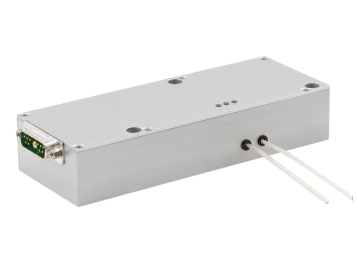
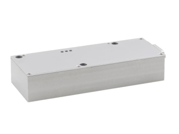
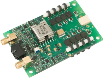
HVSW-03
带嵌入式电源的
高压、高频率普克尔盒驱动
用户手册


HVSW-03是一款专门的普克尔盒驱动,其性能针对皮秒和飞秒激光器进行了优化。主要应用于脉冲拾取和再生放大器控制。


最 大输出电压为2kV;最 大重复频率在1.5kV输出电压下可达1MHz。如果需要,还可以进行改进,使得在小于1.0kV输出电压下,其重复性能可以达到2MHz。
根据负载电容和驱动器配置,过渡时间可快至5-7ns。脉冲宽<15ns(固定),然后是100-2000ns(客户可调)。
HVSW-03提供模拟和RS-485接口。同时,还提供适用于Windows® 7的配置软件。
HVSW-03的设计紧凑(约为0.3dm3),通过底部表面进行传导冷却,并集成了高压电源(即驱动器的输入为+24V DC),这些都是额外的优势。
INTERFACE (D-SUB mixed contact connector FM11W1):


HV OUTPUT (flying leads):
Two wires, each of 70mm length
Other wire’s length and termination are available on request. Shielded output wires reducing EMI, but slightly decreasing the performance are available on request.
LEDs:
POWER (green) – LED lits steadily while device is powered.
RS485 (red) – LED is lit steady when device is in stand-alone mode (analog interface is
enabled), and blinks when device is being controlled via RS-485. In bootloader (update) mode this LED makes double blinks.
STATE (blue) – LED blinks slowly when device is in stand-by mode; it blinks fast when error (overheat) is detected; and it is lit steady when HV output is enabled.
MOUNTING AND GROUNDING:
Driver to be mounted with 3pcs M4 screws (recommended screws are DIN 912, M4x10 or longer).


COOLING:
Driver is conductively cooled through the bottom surface, which in dependence on actual heat dissipation should be attached either to massive chassis, or to heat sink or to cold
plate of the appropriate performance.
For better heat removal thermal grease or equivalent maybe used.
Safety

• Do not connect / disconnect output cables while driver is turned on• Avoid casual contacts of personnel with output cables and with the load
• Do not operate with disconnected load
• Do not turn the driver on if it was already damaged with water, chemicals, mechanical or electrical shock
• Do not self-repair the driver, there are no user-serviceable parts inside
• Driver’s input-to-output insulation isn’t a safety feature, but just functional one, so we
highly recommend to use low voltage power supply with input-to-output insulation
providing appropriate level of protection (4000VAC or 2500VAC in dependence on your application)
[Pre-configuration, optional]
1. Connect +24V DC power supply to the driver, connect driver to PC (or to another controlling device)
2. Run provided Windows ® software (or terminal software)
3. Configure the driver using provided Windows® software (or using RS-
485 commands)
4. Disconnect the driver from PC (from another controlling device)
[Operations]
1. Attach driver to the cool plate (another cooling device)
2. Connect +24V DC power supply, Pockels cell and pulse generator to the driver. Do not apply +24V DC power before the entire setup is
completely assembled
3. Turn on +24V DC power supply to power up the driver
4. Apply HV Program (pin 1) analogue voltage corresponding to the desired output voltage
5. Enable the driver using HV Enable signal (pin 5)
6. Apply Pulse signal (pin A1) with the desired pulse width and repetition rate
RS-485 interface description

RS-485 connection parameters: 57600 bps, 8 data bits, 1 stop bit, no parity. Default protocol is described in Appendix A.
Simplified protocols are available on request.

HV program – defines the amplitude of HV pulses (volts), 0V to 2000V, default value 1500V HV enable – enables the driver’s output
Gate limit – defines the maximal allowed pulse width (ns), 200ns to 2200ns, default value 2200ns
Pulse width mode (Fixed) – in this mode driver produces pulses of fixed pulse width (approximately 15ns)
Pulse width mode (Variable) – in this mode driver repeats incoming TTL signal (Pulse, A1 pin) at its output, i.e. produces pulse of variable pulse width
Triggering (Soft) – in this mode the switching of transistors is “soft” – this leads to a little bit longer risetime and falltime, but the overshoot is smaller and power consumptions (so the
internal temperature) is less
Triggering (Harsh) – in this mode the switching of transistors is “harsh” – this results in a little bit shorter risetime and falltime, but the overshoot is higher and power consumptions (so the
internal temperature) is higher
HV program mode (Default) – driver needs HV Program signal for operations via analogue interface
HV program mode (Smart) – driver doesn’t need HV Program signal for operations via analogue interface (driver uses HV program value set via software or RS-485 commands; although HV
Program signal, if applied, overrides the preset value)
Device ID (“1” by default) – driver’s ID on RS-485 bus (different ID should be assigned to different drivers if a few drivers connected to the same RS-485 bus)
Transistor temperature threshold – maximal value 100 °C, default value 100 °C Case temperature threshold – maximal value 100 °C, default value 70 °C

• Performance of the module greatly depends on load capacitance. Full
performance is achievable at load capacitance typical to Pockels cells used in laser industry (5-7pF).

• Module’s output is bipolar. This means that e.g. 2kV pulse is physically formed
by applying +1kV to one output wire and -1kV to another (see figure)

Nevertheless, all descriptions of HV output are given in terms of voltage differences. Please keep this in mind!
• Sequential pulses have reversed polarity. Since driver is built on full bridge
schema, each of two output wires varies its potential between +V and –V values (blue and yellow curves below). As a result, the voltage difference between two wires can be both positive and negative (red curve on the picture below).

• Arbitrary (random) signal applied to Pulse pin may damage the driver. Please ensure Pulse signal follows the next rules:
- Minimal allowed pulse width is 100ns
- Maximal allowed pulse width is 2000ns
- Minimal allowed distance between pulses is 100ns
- Maximal allowed distance between pulses - no limitation
- Maximal allowed repetition rate is 1MHz for standard drivers and 2MHz for high repetition rate modification.
Not every point above has the corresponding hardware protection. Please ensure the applied signals are within the allowed ranges.
ELECTRICAL SPECIFICATION

MECHANICAL SPECIFICATION


How to order?
At the moment there are two modifications different with maximal repetition rate and risetime/falltime:

Driver’s performance (i.e. the maximal possible repetition rate) depends on load
capacitance, pulse amplitude and the performance of cooling system and limited with
internal temperature (we do not recommend to exceed 80-90 °C transistor temperature) and the current consumption (we do not recommend to exceed 5A current consumption).
Performance in some typical regimes is given below:
Standard modification, ~6pF load capacitance, 2.0kV output voltage, 0.6MHz repetition rate -> cool plate temperature ~25 °C, transistor temperature ~80 °C, current
consumption ~5A
Standard modification, ~6pF load capacitance, 1.5kV output voltage, 1MHz repetition rate -> cool plate temperature ~25 °C, transistor temperature ~80 °C, current
consumption ~5A
High repetition rate modification, ~6pF load capacitance, 1.0kV output voltage, 1.8MHz repetition rate -> cool plate temperature ~25 °C, transistor temperature ~80 °C, current consumption ~5A

The present section describes RS-485, binary, master-slave protocol. Only one active master (at the same time) can be connected to the bus, and one or several (up to 254) slave nodes can be
connected to the same bus. HVSW-03 is a slave device and responds to the transactions initiated by the master. Each slave device has an unique address between 1 and 254 decimal and also
recognizes the broadcast address 0. Available bus baudrates for device are: 4800, 9600, 19200, 38400, 57600 (default), 115200. Available baudrate for bootloader: 57600.
Data packet format from the master:

A slave uses the frame format described below with the same synchronization and flag byte as the master.

A slave responds message in less than 50ms after receiving a fully initiating a transaction from a master. Master must generate a time out at least 100ms after finishing a transaction.
Common parameters / functions
0x00: Ping (read only), data length: 0 byte. A slave answers by sending a packet with no data.
0x01: Device ID (write only), data length: 1 byte, range: 1..254, default value: 1. Function sets the new device ID, which is used immediately after this write request.
0x02: Protocol version (read only), data length: 1 byte, range: 1..254. A slave returns value 1.
0x03: Device part number (read/write), data length: 2 bytes, range: 0..65535. Function sets/returns device part number.
0x04: Device serial number (read/write), data length: 2 bytes, range: 0..65535. Function sets/returns device serial number.
0x05: Hardware version (read/write), data length: 2 bytes, range: 0..65535. Function sets/returns device hardware version.
0x06: Software version (read only), data length: 2 bytes, range: 0..65535. Function returns device software version.
0x07: Device string (read only), data length: arbitrary, ASCII string. Function returns device name or description.
0x08: Bootloader control and status (read or write), data length: 1 byte, data format: bit field. Function controls the bootloader using the following format:
Write request:
Bit 0: Activate bootloader Bit 1: Clear memory
Bit 2: Boot application Read request:
Bit 0: Bootloader running (1 – yes, 0 – no) Bit 1: Memory cleared (1 – yes, 0 – no)
Bit 2: Valid application in memory (1 – yes, 0 – no)
0x09: Bootloader Stream (write only), data length: N packets of 1..255 bytes.
0x0A: Device status (read only), data length: 2 bytes, data format: bit field. Function returns device status in the following format:
Bit 0: At least one warning is present Bit 1: At least one error is present
Bit 3: Bootloader is active Bit 4: Device is ready
Bit 7: Device is “On”
0x0B: Available bus speed (read only), data length: 2 bytes, data format: bit field. Indicates availability of device specific bus speed implementations (in Bit/s)
Bit 0: 4.800
Bit 1: 9.600
Bit 2: 19.200 Bit 3: 38.400 Bit 4: 57.600 Bit 5: 115.200
Bits 6..15: reserved
0x0C: Set bus speed (write only), data length: 2 bytes, data format: bit field. Function sets bus speed.
Bit 0: 4.800 Bit 1: 9.600 Bit 2: 19.200 Bit 3: 38.400
Bit 4: 57.600 (Default Setting) Bit 5: 115.200
Bits 6..15: reserved
0x0D: Bus mute (read/write), data length: 1 byte, data range: 0-1 (0 = communication is on, 1 = communication is off). Switches off the serial communication of a device until it is switched
again using this parameter. After power on (supply voltage) device has its serial communication switched ON.
Device specific parameters / functions
0x40: High voltage (read/write), data length: 2 bytes, range: 0..2000. Sets or gets high voltage in volts.
0x41: Gate Limit (read/write), data length: 2 bytes, range: 200..2200. Sets or gets gate limit in nanoseconds.
0x42: Transistors temperature threshold (read/write), data length: 2 bytes, range: 0..1600. Sets or gets transistors temperature threshold in 0.1 °C (e.g. 800 corresponds to 80.0 °C)
0x43: Case temperature threshold (read/write), data length: 2 bytes, range: 0..1600. Sets or gets case temperature threshold in 0.1 °C (e.g. 800 corresponds to 80.0 °C)
0x44: HV enable (read/write), data length: 1 byte, range: 0 .. 1. Enables (1) or disables (0) high voltage.
0x45: Pulse width mode (read/write), data length: 1 byte, range: 0..1. Sets or gets pulse width mode (1 – fixed, 0 – variable).
0x46: Triggering mode (read/write), data length: 1 byte, range: 0..1. Sets or gets triggering mode (1 – soft, 0 – harsh).
0x47: HV Program mode (read/write), data length: 1 byte, range: 0..1. Sets or gets HV program mode (1 – smart, 0 – default).
0x60: Get sensors (read only), data length: 1 byte, range: 0..255. Returns device sensors in the following format:
Bit 0: Overtemperature error
Bit 1: Gate limit error Bits 2-5,7: reserved
Bit 6: HV fault error
0x61: Get transistors temperature (read only), data length: 2 bytes, range: 0..1600. Returns current transistors temperature in 0.1 °C (e.g. 800 corresponds to 80.0 °C).
0x62: Get case temperature (read only), data length: 2 bytes, range: 0..1600. Returns current case temperature in 0.1 °C (e.g. 800 corresponds to 80.0 °C).
0xF2: Get all monitors (read only), data length: 5 bytes. Returns all monitors in the following format: sensors (1 byte), transistors temperature (2 bytes), case temperature (2 bytes).
0xF1: Get all parameters (read only), data length: 13 bytes. Returns all parameters in the
following format: high voltage (2 bytes),gate limit (2 bytes), transistors temperature threshold (2 bytes), case temperature threshold (2 bytes), sensors and states (1 byte in the following format: Bit 0: overtemperature error, Bit 1: gate limit error, Bit 2: high voltage enable state, Bit
4: pulse width mode state, Bit 5: triggering mode state, Bit 6: HV fault error), transistors temperature (2 bytes), case temperature (2 bytes).
Examples:
A1 00 01 00 FC – ping device with ID = 1 (answer: A0 00 00 48)
A1 00 01 61 DC – get transistors temperature for device with ID = 1 (answer: A0 02 00 EF 00 5F – temperature is 23.9 °C)
A5 02 01 40 E8 03 EC - set high voltage to be 1000Vfor device with ID = 1 (no answer)


 服务热线:
服务热线: